MelonTools hardening device
There’s a type of processing called ElectroSpark Alloying (ESA)/ ElectroSpark Deposition (ESD), which is an incremental electrospark processing. Using erosion of electrode and electric discharge you can build an incremental layer on metals, which has properties established overhand, often different than those of base material. Using this method, you can fill holes, by using electrode of the same properties same as the base material, but most widely used is incremental electrospark hardening.
Distinctive feature of electrospark coating is its specific non-digestive structure — it remains white. Top layer is formed by affecting locally with high temperature and big pressure. Values of main parameters of electrospark processing are as follows:
- pressure of the impact wave from the electric spark equals (2-7) * 103 GPa,
- temperature gets up to (5-40) * 103 st. C°
During the process of creating layers with the electro spark processing there are following physical phenomena: increase in intensity of electrostatic field while drawing the electrodes nearer, electrical breakdown, ionization of gas in aperture (with gas or vacuum), creation of plasma channel, luminous and heat radiation and vaporization, short circuit of electrodes, impacting of electrodes, erosion of cathode and anode, transfer of material, forming of the coating, diffusion and solidification.
Using electrodes based on tungsten carbide with cobalt (WC-Co) you can get a specific layer, non-digesting, white layer that has a large abrasion resistance.
The top layer created with ESD/ESA consists of (when using WC-Co electrodes):
- white, hard, non-digesting layer,
- heat affected zone,
- base material.
Everyone knows how it works, create patents everywhere, and, of course, sell devices for creating such layers.
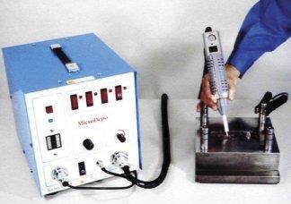
Looks interesting:
The devices are quite bulky (14-30kg), with high power, and quite dangerous (high currents, voltage, etc.).
The layer created with ESA/ESD, and WC-Co electrodes (Co: 5-10%) has hardness of about 600-650HV, and it’s abrasion resistance can exceed the abrasion resistance of base material by hundreds of times (in case of alloy of titanium, aluminium, and soft steel). The thickness of the layer may be around 5-100 μm. Thanks to tungsten carbide WC, the abrasion resistance may be considerably higher even than hardened low-alloy steel (750HV).
Someone saw a business, and started producing devices for hobbyists. Those devices have less power, are cheaper, and are a bit safer. You just had to have a look at what the electric current connected to metal does:
Looks the same as on the movie above! From there it was close to creating “devices same as those used in industry”. A bit of marketing, and it all started to turn:
And it began, an outbreak of devices intended for hobbyists:
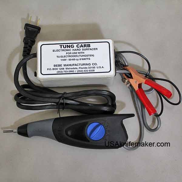
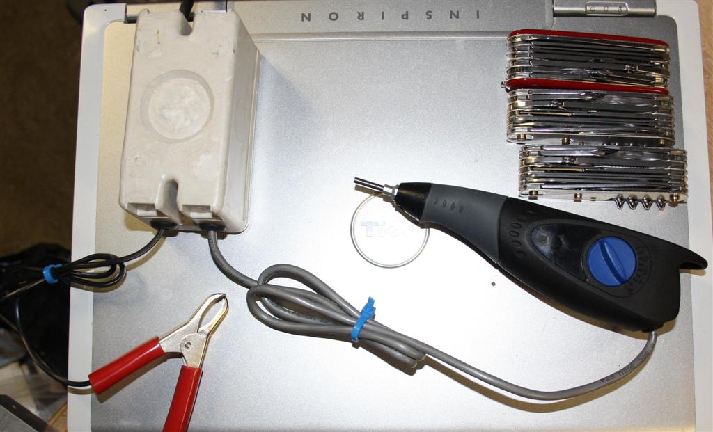
Those “devices” give the same looking layer as the bulky, heavy, awkward industrial “ugly things”, THEY HAVE TO EFFECT THE COVERED METAL THE SAME WAY! This looks especially effective on titan:
Everything would be ok, but I’m a bit concerned by the low power of “hobbyist devices”, which sometimes is 60W (-15W for the drive, so the power supply only gets about 45W), opposed to 500-1000W industrial whoppers.
Why? I wanted to create a “hobbyist device” that will give a similar characteristics of the top layer as the industrial devices, with a lower power, but, what’s most important, SAFE for the user.
After about a year of reading, watching, building, disassembling, plotting, and breaking, something emerged. I only had to compare with “hobbyist devices” from the store, and DYI devices from Youtube.
I’ve used heat threated 4H13 steel (I used my Pocket Tools, that were badly engraved, and hardened to about 50HRC), and a person who heard about such processing and device for the first time (thanks Kiścień!). Layers were imposed in a similar way, in two stages. I’ve also used a bit of Kuba’s scientific knowledge (doing metallographic microsections, and microscopic photos).
Outcomes are very interesting:
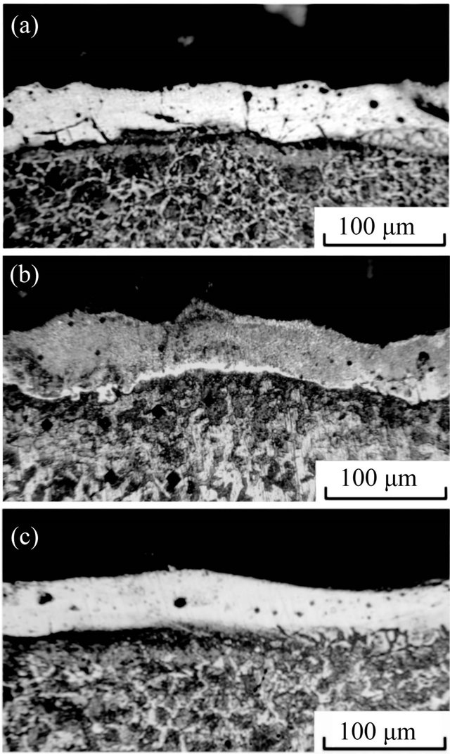
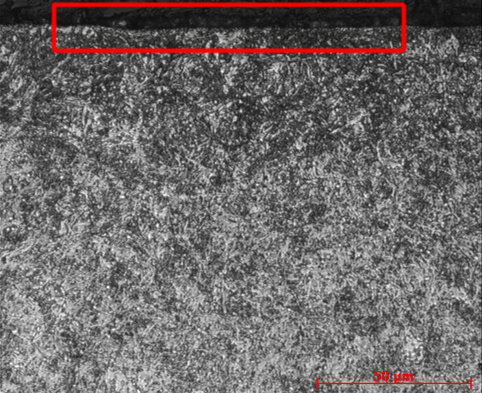
First sample, done with the “hobbyist device”:

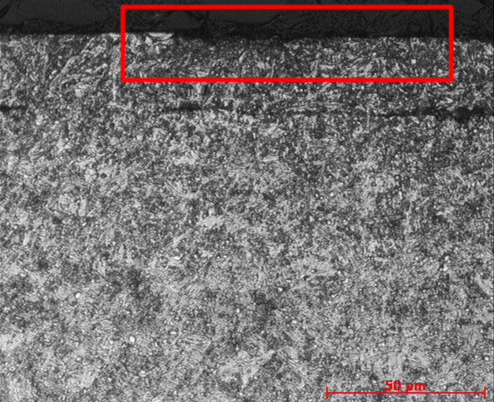
As you can see, there is no white layer, only thing visible is the heat affected zone. The white layer is responsible for the abrasion resistance, and corrosion resistance. The harder and thicker it is, the more it protects the material beneath it. Without the white layer, the resistance is considerably (many times) lower.
Second sample: a self-made device borrowed from a good soul from www.knives.pl:
Same as above.
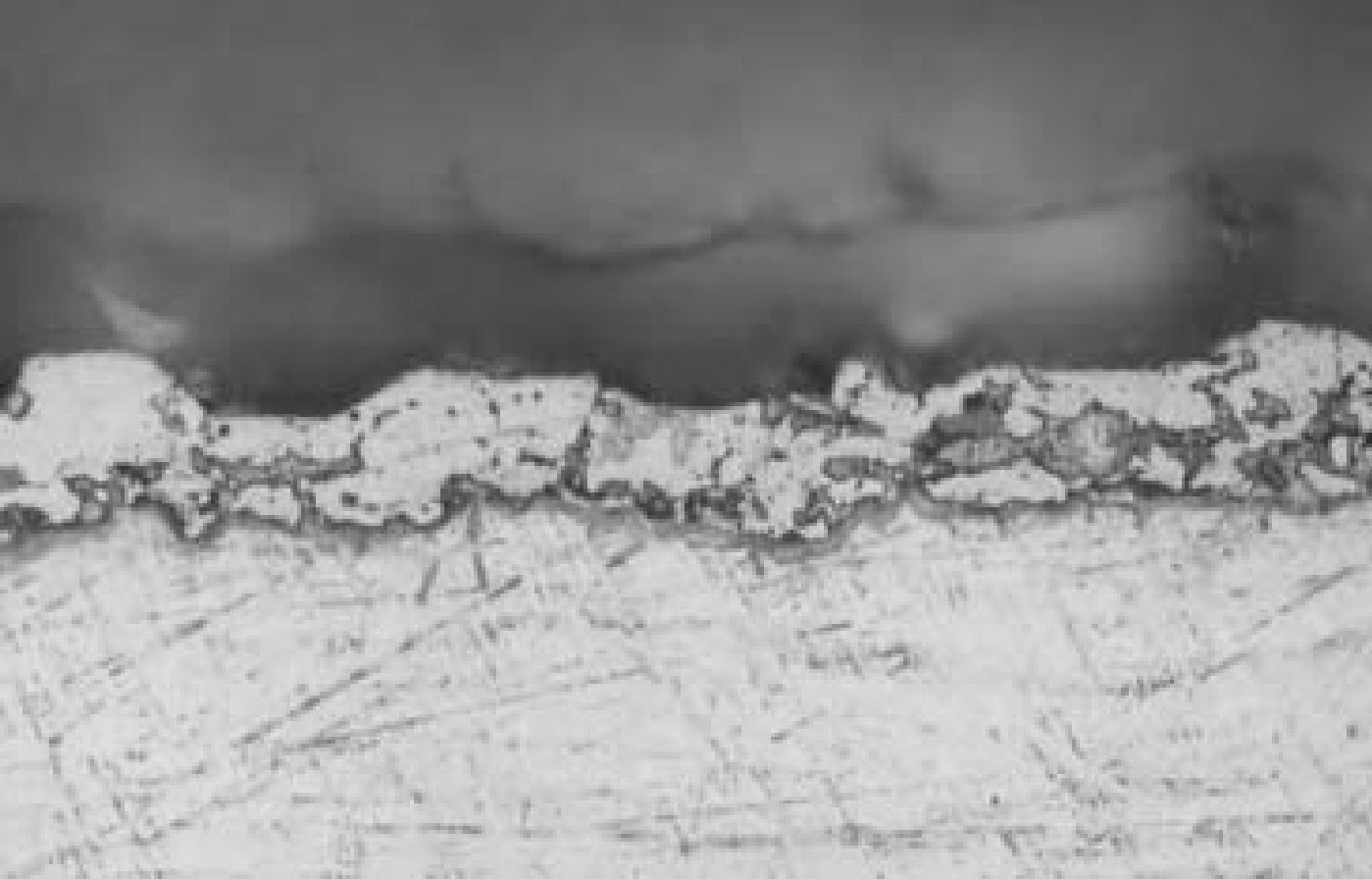
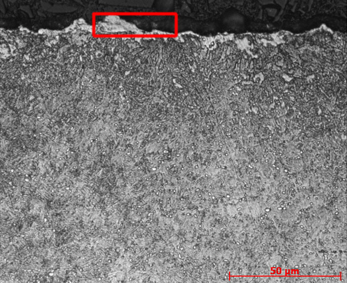
Third sample: top layer after upgrading (!) it with stabilized 400W power supply:
As you can see, there’s still no white layer. The sample looked the same after adding capacitors.
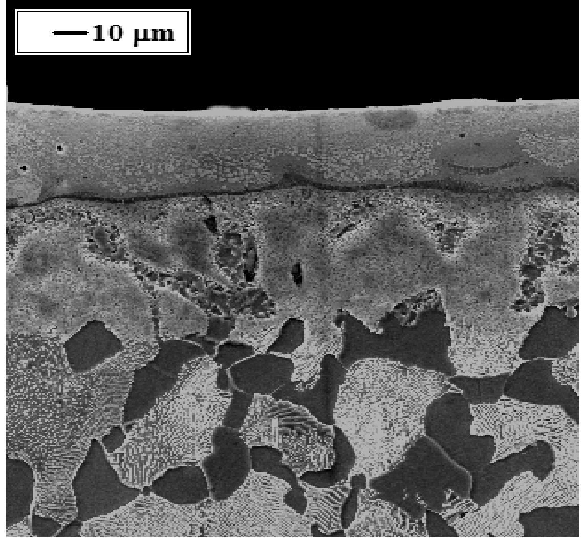
Fourth sample: the device I made earlier, but with power over 400W. When grabbing the electrodes, you could kill 2-4 people at once (!). I was very scary to do.
As you can see, the white layer appeared, it’s non-digesting (hard from WC-Co), but very small in comparison to the one done with industrial devices on the photos from the top. BUT IT’S THERE! So the abrasion resistance is a lot better than without it.
Fifth layer: the device I’ve made now — with voltage below 50V, and power below 100W:
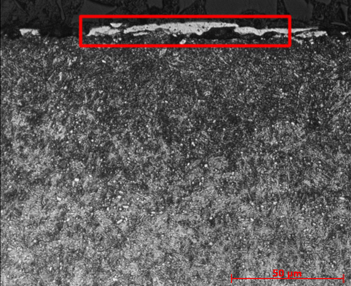
As you can see the non-digesting layer is thicker (over 5 μm), and, with that, the abrasion resistance is further increased!
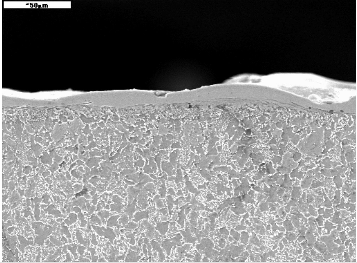
After suggestion from one of my colleague, I’ve added amplifier to my device (as a separate module) and with voltage below 100V, and power above 150W I got something like this:
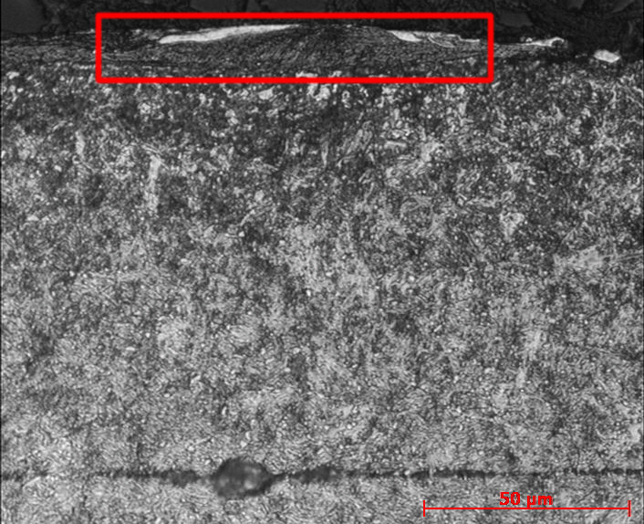
As you can see, the white layer is even thicker (5-10 μm) and steady. That’s what I wanted! The steady layer will be a good protection, it’s going to be harder to “pry”, and “flake off” during exploitation. With the same hardness of the white layer, non-digesting, with the increase of it’s thickness, it’s abrasion resistance also resists.
WAIT, WAIT!
If the “hobbyist devices” don’t cause of creation of the white layer, why does tools it’s been used on are longer lasting.
A bit of theory:
The forming of surface during electrospark embeding (ESD/ESA) is done by layering craters created by erosion of foundation, and ridges from transporting mass from the hard electrode.
The local temperature during this processing is above boiling point of electrodes (material and hard electrode). The high speed of heat dissipation causes creation of close-grained imbalanced structures with addition from the hard electrode.
With sufficient power of devices, and ADEQUATE voltage current characteristic (it’s not enough to use direct current power supply, the power source needs to be altered a bit) you can create the white layer, non-digesting and hard. AND THAT’S WHAT IT’S ALL ABOUT!
But, if the power is not big enough, bad voltage current characteristic (even if the power is right) the process is crippled, it’s not going as described in scientific publications, and the marketing somehow forgot to mention about this. Besides, who checks the outcomes of “hobbyist devices”, everything has been described in scientific publications! Small toys work the same as the large ones, they’re just cheaper!
What if, however, too little material from the hard electrode is transferred in electric arc to create white layer, hard and non-digesting? Then, the close-grained structure is responsible for hardening of the top layer, imbalanced, with addition of hard electrode, and detonative strengthening (but again, the strengthening is not as big as described in literature). Same as with hardening metals with laser beam – the order of magnitude is not the same, but the mechanism is similar.
That is why I daresay that my equipment works better, creating thick enough white layer, non-digesting, with WC-Co, and that layer, created using my device, will last much longer than layers created with “hobbyist devices” available in stores today.
But it looks so pretty on titan, after processing with Carbidizer!
Better than on steel, after Carbidizer the surface is very nice! And what, does such “hobbyist” Carbidizer processing is not enough?
Titan is a low-alloy metal; it evaporates easier during electric discharge (in comparison to steel), creating beautiful craters (that’s why it’s harder to achieve visually appealing layer on steel), and strain hardened (deformed) layer, with traces of tungsten, carbon, and cobalt. However, that is not enough to create the white layer!
Someone enlightened me (BrrKnives), that it’s really not important how much volts we’ve got, if we are in occlusion or very close, the voltage drops to couple of volts. When creating layers with ESD/ESA, and hand layering those unstable states are in quite low voltage.
Therefore, I daresay:
- if someone is connecting 240V with separating transformer,
- impulse power supply with any voltage,
- STABILIZED power supply (I’ve started with one of those),
- small and large capacitors,
- any other crap resembling its behaviour more or less to an electric chair,
the look of the surface is going to be similar (although there will be singular large craters if starting with large voltage). The true differences will be visible under microscope, or during the abrasibility test – this will show how much the equipement (and the top layer on it) is worth.
If we plunge into voltage current characteristic (and modify it) of electric source with electric receiver, like the electric arc between the coated piece, and electrode: we get into wishful thinking zone.
But why did I write all this?
Because I’m happy like a child that I managed to build such a device (Poles can do it!). I hope I will mage to mass produce it with CE certification — which none “hobbyist devices” available in EU have.
I give my thanks to BrrKnives, and Alek (I’ve never seen him, I didn’t even spoke to him, but he’s a good man!), Kuba (photos), Lola (for being there), and Lilu (for calmly bearing with all my “hijinks”). Without them this device would not be created, I just got together all the pieces I got from them :).
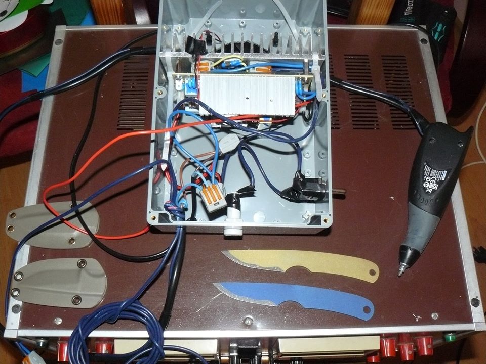
I’m happy to be able to present to you the production version of the Melondizer:

- MELONDIZER mod.1A
- MELONDIZER mod.1
Why two devices? It turned out that the base version is “too weak”, and gives satisfying results only on alloys of titan (and light alloys). To increase the abrasion resistance on titan, and get satisfying results on steel, you need to connect additional device to Melondizer mod.1 — and amplifier (Melondizer mod.1A). The manuals are ready, I print them and can brag with the first polish hardening device with CE.
For hardening framelock and linerlock in folders.
I also thank Jacob Hubiszowi for translating this entry into English.
Bibliography:
- Method and apparatus for electrospark alloying US 6417477 B1
- Sergey A. Pyachin, Sergey V. Nikolenko, Alexander A. Burkov*, Nikolay A. Suy: Electrospark Coatings Based on WC-Co Alloys with Aluminium Oxide and Carbon Additives
- moldmakingtechnology.com/
- Radek: Wpływ obróbki laserowej na właściwości przeciwzużyciowych powłok elektroiskrowych
- Radek: Badania eksploatacyjne bijaków stalowych obrobionych elektroiskrowo
- Rozmus, J. Kusiński, M. Blicharski, Ł. Major: Laserowo odkształcona warstwa wierzchnia stopu tytanu Ti6Al4V
- Napadałek, A. Szarzyński: Umacnianie warstwy wierzchniej stopu tytanu WT3-1 falą uderzeniową generowaną impulsem laserowym – zjawiska fizyczne i wybrane własności
- usaknifemaker.com
- multitool.org
- ecosknives.com